Monthly Archives: April 2023

Wearable Electronics with Screen-Printing

Although screen-printing methods are commonly useful for making T-shirts, manufacturers are now experimenting with the same technique for making flexible and wearable electronics. The easy manufacturing technique is also quite inexpensive.

The tech industry is increasingly promoting the popular use of flexible, wearable electronics. This promotion includes fitness trackers and smartwatches, which consumers are adopting widely. However, there is a huge challenge in making these devices—the process is rather error-prone, complex, and expensive.

Another challenge that manufacturers of such flexible, wearable electronics face are the high cost of raw materials. As the materials these devices require for the flexible sensors and displays are relatively new, they are expensive to produce in large quantities. Therefore, manufacturers find it difficult to produce high-quality and affordable devices.

The complexity of the manufacturing processes for these devices is another major challenge. The process of manufacturing these flexible, wearable electronic devices requires various steps, involving the printing of thin-film transistors, creating flexible substrates, and assembling the final device. Each step requires the execution to be at a high level of accuracy and precision. This not only increases the risk of errors but is also difficult to achieve.

In contrast, the screen-printing process, or the silk screen printing process, is a technique that is in use for centuries now. The process requires pushing ink through a mesh screen or stencil and depositing it on a surface. A non-permeable material blocks off sections of the mesh screen to leave open only the desired design. This allows ink to pass through only the openings.

Not only does the above process require very inexpensive and minimal material, but it is also incredibly simple as well, and anyone can do it by hand. So far, manufacturers of T-shirts have used this process, but now it has inspired a research team from Washington State University also. They experimented with the technique to check out its suitableness for printing flexible, wearable electrodes among other electronic components.

The team started by printing multiple layers of polyethylene glycol and polyimide mixture on a glass slide. They interspersed this printing with a conductive, patterned layer of silver. After completing the printing process, they peeled off the screen-printed material from the slide, affixing it to the body or fabric. Then they formed a serpentine, highly deformable pattern of electrodes, which could stretch to more than 30% of its regular size, and bend at up to 180 degrees without any damage.

The researchers created a wearable, real-time, wireless, electrocardiogram monitoring device using their new method, and put it to the test. They developed an algorithm to process the sensor data from the flexible printed circuit and the printed electrodes. Their device could accurately calculate respiratory rates, heart rate, and its variability metrics. According to the researchers, the variability metrics could have clinical applicability in the detection of arrhythmia.

The main advantage of the approach by the team is they can easily scale up their technique. Therefore, they can use the same technique for creating a single device or for mass-producing a commercial wearable. Moreover, the same technology is useful even beyond medical devices, such as in producing fitness trackers and smartwatches.

Nanowire Sensors

The Center of Excellence at the Australian Research Council for TMOS or Transformative Meta-Optical Systems, has announced the development of a new type of sensor. This is a minuscule sensor made for detecting nitrogen dioxide. They claim it can protect the environment from pollutants that vehicles typically release. These pollutants can cause acid rain and lung cancer.

According to the researchers, the sensor consists of an array of nanowires. The array occupies a square of only a fifth of a millimeter on each side. That means a silicon chip can easily incorporate the sensor.

The researchers have published their findings in the latest issue of Advanced Materials. They have described their sensor as not requiring any power source, as it has a built-in solar-powered generator to run it.

According to the researchers, by incorporating the new sensor into a network benefits the Internet of Things technology, as the sensor has low power consumption, low system size, and is inexpensive. They claim that it is possible to install the sensor into a vehicle. If the sensor were to detect dangerous levels of nitrogen dioxide from exhaust emissions, it will sound an alarm and send an alert to the owner’s phone.

The researchers feel this device is only a beginning, as they can adapt the sensor for the detection of other gases like acetone, which can lead to the design of a ketosis breath tester. Such a non-invasive tester can help to detect diabetic ketosis, saving countless lives.

This is an important development, as existing detectors require a trained operator and are bulky and slow. The new device, in contrast, detects gases instantly, measuring less than one part per billion of the gas. The prototype from TMOS even has a USB interface, allowing it to connect to a computer.

Belonging to the NOx category of pollutants, Nitrogen dioxide is highly dangerous to humans even when present in very small concentrations. Moreover, it contributes to acid rain, cars generate it commonly as a pollutant, and gas stoves can also generate it indoors.

Common to the fundamental construction of a solar cell, the nanowire sensor also consists of a PN junction, but in the shape of a nanowire. Sitting on a base, the nanowire is a small hexagonal pillar that has a diameter of about 100 nanometers. The complete sensor has a thousand of these nanowires in an ordered array, with the spacing between them measuring 600 nanometers.

Made from Indium Phosphide, the sensor has its base doped with zinc, forming the P part, while the tip of the nanowires forms the N section, as the researchers have doped it with silicon. Separating the P and N sections, the middle part of each of the nanowires remains undoped, constituting the intrinsic section.

As in the case of a solar cell, any light falling on the device causes the flow of a small current between the N and P sections. If nitrogen dioxide is present and touches the intrinsic middle section, there will be a dip in the current. This is due to nitrogen dioxide being a strong oxidizer that removes electrons.

Batteryless Microcontrollers for IoT

Ten years ago, IBM predicted the world will have one trillion connected devices by 2015. However, as 2015 rolled by, the world had yet to reach even 100 billion connected devices. The major problem—a trillion sensors mean at least a trillion batteries.

Although a significant problem, it did not make economic sense. Everyone was expecting the IoT technology to bring on a large value-addition, that of range. They expected IoT to bring the Internet to remote corners of the world, thereby interconnecting vast areas with IoT sensors and their information-gathering powers. Therefore, the internet and its incredible power would be visible in various places like large farms, factories, lumbering operations, construction sites, and mining operations, with enormous coverage and decentralized operations.

Typically, sensors collect data for IoT networks, which distribute it for processing and analysis. If sensors require batteries for operation, it places a severe restriction on the number of sensors that a network can use. This, in turn, goes on to defeat the entire point of having IoT in the first place.

For instance, consider a large-scale agricultural operation. IoT can bring major value addition to such a business through its coverage. By deploying multiple sensors across the entire operation, it is possible to access valuable information capable of generating highly actionable insights. Now consider the recurring cost of replacing or maintaining the huge number of batteries every year—making the proposition less compelling very quickly.

Not only would the resources, cost, and manpower, for replacing or maintaining the batteries on all the sensors be astronomical, but they would also easily surpass any possible savings that the system would likely bring.

According to an estimate, a trillion sensors would need 275 million battery replacements every day. This, assuming every battery deployed in the IoT network reached its claimed life of ten years. The next hurdle is even worse—discarded batteries poisoning the environment.

The above problem has resulted in sensors and microcontrollers getting more efficient and cheap. Modern sensors are now extremely reliable, consuming minuscule amounts of energy. Batteries have also improved, with the industry exhibiting robust batteries with higher energy density and longer life. However, the future of microcontrollers and IoT sensors needed to be batteryless. This led scientists and engineers to develop energy harvesting technologies that could eliminate the battery from IoT altogether. 

Energy harvesting is the technique of scavenging power from the surroundings, which has many forms of it—heat energy, electromagnetic energy, vibrational energy, and so on.

Considering that modern microcontrollers for IoT need only a few millivolts to operate, many are developing energy harvesting technologies as a potential power solution that can replace batteries.

This has given rise to self-powered microcontrollers in the market. For these MCUs, batteries impose no restrictions, as they harness their own energy from the environment. They use a number of harvesting technologies based on various power sources and kinds of materials—piezoelectricity, triboelectricity, and RF energy harvesting being the leading contenders in the category. Therefore, with energy harvesting powering microcontrollers, IoT can once again begin to chase the magic figure of one trillion interconnected devices.

Tiny Batteries Drive Microbots

Microbots are mobile robots, with characteristic dimensions below one micrometer. They are a part of the bigger family of common larger robots and a growing number of smaller nanorobots. In fact, the nature of microbots is common to both their larger and smaller cousins. Being autonomous, microbots use their onboard computers to move in insect-like maneuvers. Often, they are a part of a group of identical units that perform as a swarm does, under the control of a central computer.

With their insect-like form being a common feature, microbots are typically cheap to develop and manufacture. Scientists employ microbots for swarm robotics, using many of them and coordinating their behavior to perform a specific task. Combining many microbots compensates for their lack of individual computational capability, producing a behavior resembling that of an anthill or a beehive where insects cooperate to achieve a specific purpose.

With the field of microbotics still growing, microbots have a long way to develop further. Researchers are working with these devices, and they are investing their money, time, and effort in improving their capabilities.

With each new iteration, scientists are empowering microbots with more processing power, newer modes of locomotion, a larger number of sensors, and expanding their storage methods while providing them with newer techniques of energy harvesting. Recently, there has been a big breakthrough in tiny batteries that can help microbots drive further than ever before.

Generating a 9 VDC output, these tiny batteries are capable of driving motors directly. They stack multiple layers while turning components into packaging.

Several universities and a battery corporation have joined hands in creating the tiny batteries, a novel design that not only produces a high voltage but also boosts its storage capacity.

To unlock the full potential of microscale devices such as microbots, batteries must not only be tiny, they must also be powerful. According to the team that developed the tiny battery, its innovative design uses an improved architecture for its electrodes.

However, this was an unprecedented challenge. As the battery size reduces, the packaging begins to take up more of the available space, leaving precious little for the electrodes and the active ingredients that give the battery its performance.

Therefore, in place of working on the battery chemistry, the team started to work on a new packaging technology. They turned the negative and positive terminals of the battery into actual packaging, thereby saving considerable amounts of space.

By growing fully-dense non-polymer electrodes and combining them with vertical stacking, the team was able to make micro batteries that do not require carbon additives for electrodes. This allowed the micro batteries to easily outperform competitive models in capacity and voltage.

According to the team, limitations of power-dense micro- and nano-scale battery design were primarily due to cell design and electrode architecture. They have successfully created a microscale source of energy that has both volumetric energy density and high power density.

The higher voltage helps to reduce the electronic payload of a microbot. The 9 VDC from the tiny battery can power motors directly, bypassing energy losses associated with voltage boosting, allowing the small robots to either travel further or send more information to their human operators.

Batteries and Supercapacitors

In the past, only mission-critical devices had them. Now, a wide range of electronic applications demands backup power solutions. These applications include consumer, commercial, and industrial end-products. Of the several options available, the most energy-dense solution is that offered by supercapacitors, acting as energy reservoirs during interruptions of the main supply. Typically, this occurs during an outage of the mains power, or during swapping out batteries.

Although they are versatile, supercapacitors present challenges in design. This is due to their capacity to provide only 2.7 VDC. Potentially, this means adding multiple supercapacitors, along with the necessary cell-balancing circuitry, and voltage converters for step-up and step-down for supplying regulated power to the power rail operating at 5VDC. The solution is a nuanced and complex circuit, which not only takes up excessive board space but is also relatively expensive.

Comparing them with batteries can explain why supercapacitors offer many technical advantages for compact, low-voltage electronic applications. Supercapacitors help in designing simple, elegant solutions for powering a rail operating at 5VDC using only a single capacitor in combination with a buck/boost reversible voltage converter.

Modern electronic devices often need uninterruptible power as a critical element to provide a satisfactory user experience. The absence of a constant power source can not only stop the electronic product from operating, but it can also lead to vital information loss as well. For instance, a personal computer operating from mains power will lose the information contained in its volatile RAM during a power outage. Similarly, important blood glucose readings in the volatile memory of an insulin pump may be lost while replacing its batteries.

It is possible to prevent this from happening by including a backup battery. Not only will the battery store energy, but it can also release it during the failure of the main source of power. Currently, devices typically use lithium-ion batteries, as these are mature technology, offering very good energy density. This allows relatively compact devices to offer considerable backup power for relatively extended periods.

Irrespective of their base chemistries, batteries offer distinctive problematic characteristics under specific circumstances. Not only are they relatively heavy, but they also take relatively long times to recharge, which may be problematic in areas with frequent power outages. Moreover, it is possible to recharge the cells only a limited number of times, thereby increasing maintenance costs. In addition, batteries often include chemicals that can introduce environmental and safety hazards.

The supercapacitor, or ultracapacitor, offers an alternative solution. Technically, the supercapacitor is a capacitor with an electric double layer. Manufacturers construct supercapacitors using electrochemically stable, symmetric positive and negative carbon electrodes. They separate the electrodes by an ion-permeable separator that is insulating and use a container that they fill with an organic salt/solvent electrolyte.

Supercapacitor manufacturers design the electrolyte to maximize electrode wetting and iconic conductivity. The combination of the minuscule charge separation and high surface area of activated carbon electrodes results in the very high capacitance of the supercapacitor, as compared to the capacitance of regular capacitors.

The reliance on electrostatic mechanisms to store energy makes the electrical performance of supercapacitors more predictable than those of batteries.

Customer Project: Dual Power Supply

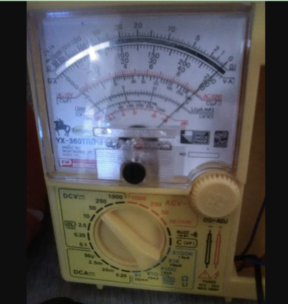
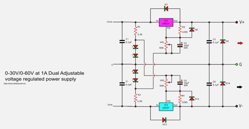
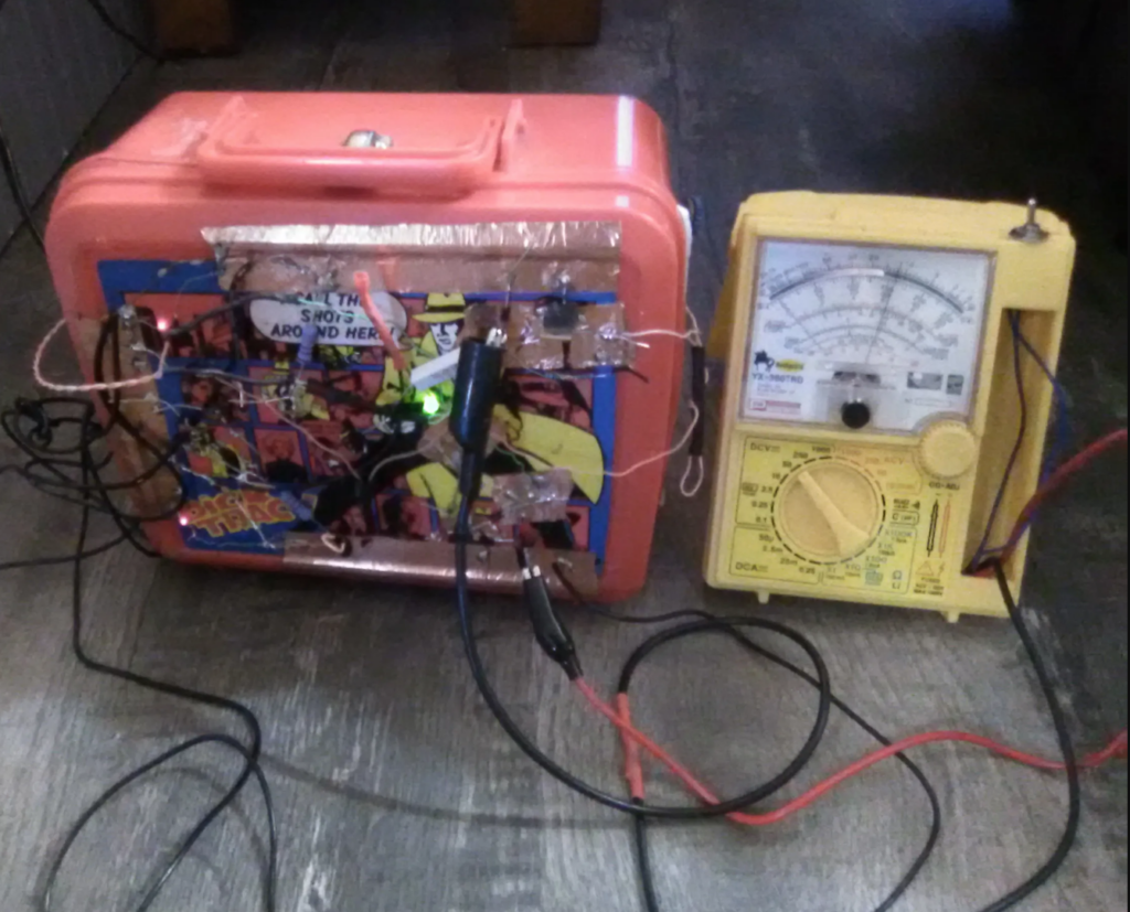
Our customer, Justin, purchased some parts for a dual power supply project and it works great! He said it can output up to +/-30v or 0-60v. It uses two 32vdc printer power supplies instead of a transformer which is inside the case.

See the pictures below of his completed project. Nice job, Justin!

Green and Wireless IoT

IoT or the Internet of Things presents devices with a collection of components for connecting various systems, software, and people via the Internet technology. Of these, the communications network is a crucial component, and the IoT wireless technology enables this. The communications network acts as the gateway between a software platform and an IoT device.

In many industries and even in daily life, the IoT is already displaying a major impact. IoT basically connects a variety of smart objects of different shapes and sizes, facilitating data exchange between them. These objects can be self-driven cars with sensors that can detect road obstacles, home-security systems, and temperature-controlled industrial equipment. Furthermore, the interconnection is often over the internet and other communications and sensing networks.

Several thin-film device technologies are emerging. They typically rely on alternative semiconductor materials, which can be nanocarbon allotropes, printable organics, and metal oxides. As suggested by an international team, KAUST, these could contribute to a more environmentally sustainable and economical Internet of Things.

By the next decade, expect the ballooning hyper-network of IoT to reach trillions of devices. This will boost the number of sensor devices this platform deploys.

The present IoT technology relies heavily on batteries to power sensor nodes. Unfortunately, batteries require regular replacement. That makes them environmentally harmful and expensive over time. Moreover, the present global production of lithium for battery materials may be unable to keep up with the increasing numbers of sensors and their energy demand.

An alternative approach relies on energy harvesters and wirelessly powered sensor nodes for achieving a more sustainable IoT. These energy harvesters may be radio-frequency-based, photovoltaic cell-based, or use other technologies. Such power sources could readily enable large-area electronics.

The KAUST team has assessed the viability of several large-area electronic technologies for their potential of delivering wirelessly powered IoT that is more eco-friendly.

Relative to conventional technologies based on silicon, large-area electronics are now emerging as an appealing alternative. This is because of the significant progress that solution-based processing is making, resulting in easily printable devices and circuits on flexible, large-area substrates. It is possible to produce them at low temperatures and on a variety of biodegradable substrates like paper. That allows more eco-friendly sensors in comparison to counterparts based on silicon.

The KAUST team has, over the years, been developing a wide range of radio-frequency-based electronic components. These include organic polymer and metal oxide-based semiconductor devices commonly known as Schottky diodes. For making wireless energy harvesters, these devices are very crucial, ultimately dictating the cost and performance of sensor nodes.

The KAUST team has been making key contributions that have included scalable methods of manufacturing RF diodes for harvesting energy. These diodes easily reach the 5G/6G frequency ranges. According to the team, these technologies are providing the necessary building blocks to sustain a trend towards a more sustainable way of powering the future billions of sensor nodes.

Currently, the team is investing in the integration of low-power monolithic devices with sensors and antennae for showcasing their true potential.

Electronically Commuted Motors — Higher Efficiency

Restaurant owners have long been facing operational challenges. These include high energy costs, limited kitchen space, and equipment downtime. For addressing these challenges and improving restaurant productivity, the owners have turned to commercial kitchen equipment. Most of such kitchen equipment has an electric motor at heart, whose performance dramatically impacts how the equipment operates and how it mitigates the above challenges.

It is imperative that owners increase their productivity while reducing their costs, considering their profit margin usually falls between three and five percent. This requires a clear understanding of the connection between the motor and the equipment. Doing so not only reduces the operating costs but also ensures a smoother running operation.

Energy costs happen to be a major concern in the restaurant industry. Commercial kitchen equipment is uncommonly hard on the electricity bill, being typically robust and energy-intensive. According to the US Energy Information Administration, consumption in restaurants is typically three times more per square foot than any other comparative commercial enterprise. This is because restaurants use specialized equipment that has a high power demand, and they operate for extensive hours, thereby consuming huge amounts of energy.

Therefore, purchasing and using high-efficiency, higher energy star-rated restaurant equipment is one of the easiest ways to improve the bottom line. However, as a motor is at the heart of each piece of equipment, it offers a greater choice. In fact, restaurant operators can improve on this further by taking a proactive approach and selecting equipment that has an electronically commuted motor or ECM. They can even consider retrofitting existing equipment with ECMs for a more favorable option.

The reason for the above decision is that an ECM operates more efficiently as compared to what a traditional induction motor does when running restaurant equipment such as ovens, walk-in coolers, mixers, and fryers. Depending on the use cycle, equipment with ECM technology can save more than 30% in annual energy costs. This improves the bottom-line savings and improves the profitability of a restaurant.

A microprocessor and electronic control help to run an ECM. Compared to regular induction motors, this arrangement offers higher electrical efficiency. It also offers the possibility of programming the precise speed of the motor. Moreover, ECMs can maintain high efficiency across a wide range of operational speeds.

Apart from the higher efficiency, ECMs are precise and offer variable speeds, which in fans means an unlimited selection of airflow. A properly maintained airflow during changes in the static air pressure brings important benefits to the restaurant, especially for its hood exhausts and walk-in coolers. The higher efficiency of ECMs leads to reduced heat in the refrigerated space, thereby reducing the equipment runtime.

Forward-thinking original equipment manufacturers are re-engineering their designs and products to include ECMs for delivering smaller and more versatile equipment. Compact motors such as ECMs, are gaining wider recognition and appreciation as they improve the power density of their equipment. Compared to equipment with traditional induction motors, those using ECMs offer the same output, but with a much smaller footprint and lower weight.

Industrial Automation with Single-Pair Ethernet

Efficiency is the fundamental concern for the successful implementation of any factory automation solution. For this, it is necessary to implement control and power components that consume the least possible amount of energy over their lifetime. However, for the actual realization of those savings, it is necessary for proper installation of the system.

This is where the advantages of the SPE or Single Pair Ethernet technology really come across. The technology transfers power and data over the same thin-wire cable. Not only does this save installation costs up-front, but it takes much less to maintain and upgrade the system over time. Phoenix Contact offers their ONEPAIR series for standardized SPE solutions. The ONEPAIR series has two main types of connectors, and they each serve a specific application.

In numerous industries and fields, the IP20 connectors and patch cables enable effective data transmission. This includes building and factory automation, where it is common to achieve a transmission rate of 1 Gbps for a distance of 1000 meters.

The other is the M8 device connectors, rated at IP67. They can transmit power and data safely and quickly from the OT to the IT. This is a new standard in compact connections, which can withstand harsh environments.

SPE or single-power Ethernet is high-performance, parallel transmission of power and data via Ethernet over a single pair of wires. The technology typically carries data and power through PoDL or Power over Data Line starting from the sensor and carrying through right up to the cloud. For barrier-free networking of a wide range of connectors, cables, and components, it is necessary to deploy connectors with standardized pin patterns. For this, Phoenix Contact offers standard connectors, ranging from IP20 to IP6x.

Apart from being ideally suited for a wide range of applications, the SPE is the basis for all Ethernet-based communication. Not only does it enable smart device communication, but it also opens up newer fields of application. SPE has great transmission properties, can span long distances, and optimally supports future-proof network communications. With a trend for miniaturized, resource-conserving devices, SPE offers space-saving cables and electronics.

SPE brings many benefits to its users. It can provide transmission speeds of over 10 Gbps over a single pair of wires. This helps to reduce data cabling while avoiding media breakdowns and device failures, from the field to the cloud. The user has the freedom to establish networking with a consistent structure base of Ethernet, eliminating the need for gateways. With SPE, the cabling is easier and saves time, as the user needs to guide and connect only two wires. They can use the 10Base-TIL standard Ethernet cabling for ranges up to 1000 meters.

The IEEE 802.3 defines the SPE standards. Presently, there are five standards for different transmission speeds and distances. Further standards are under discussion. The IP20 compact male connector series from Phoenix Contact are in accordance with IEC 63171-2 and are ideally suited for building and control cabinet cabling. The M8 or IP67 contacts from Phoenix Contact are in accordance with IEC 63171-5, providing robust and industrial-grade connections.