Category Archives: Circuit Boards & Breadboards

Why Use a Multi-Layer PCB?

Although a multi-layer PCB is more expensive than a single or double-layer board of the same size, the former offers several benefits. For a given circuit complexity, the multi-layer PCB has a much smaller size as compared to that a designer can achieve with a single or even a double-layer board—helping to offset the higher cost—with the main advantage being the higher assembly density the multiple layers offer.

There are other benefits of a multi-layer PCB as well, such as increased flexibility through reduced need for interconnection wiring harnesses, and improved EMI shielding with careful placements of layers for ground and power. It is easier to control impedance features in multi-layer PCBs meant for high-frequency circuits, where cross talk and skin effect is more prominent and critical.

As a result, one can find equipment with multi-layer PCBs in nearly all major industries, including home appliances, communication, commercial, industrial, aerospace, underwater, and military applications. Although rigid multi-layer PCBs are popular, flexible types are also available, and they offer additional benefits over their rigid counterparts—lower weight, higher flexibility, ability to withstand harsh environments, and more. Additionally, rigid flex multi-layer PCBs are also available, offering the benefits of both types in the same PCB.

Advantages of a Multi-Layer PCB

Compared to single or double-layer boards, multi-layer PCBs offer pronounced advantages, such as:

  • Higher Routing Density
  • Compact Size
  • Lower Overall Weight
  • Improved Design Functionality

Use of multiple layers in PCBs is advantageous as they increase the surface area available to the designer, without the associated increase in the physical size of the board. Consequently, the designer has additional freedom to include more components within a given area of the PCB and route the interconnecting traces with better control over their impedance. This not only produces higher routing density, but also reduces the overall size of the board, resulting in lower overall weight of the device, and improving its design functionality.

The method of construction of multi-layer PCBs makes them more durable compared to single and double-layer boards. Burying the copper traces deep within multiple layers allows them to withstand adverse environment much better. This makes boards with multiple layers a better choice for industrial applications that regularly undergo rough handling.

With the availability of increasingly smaller electronic components, there is a tendency towards device miniaturization, and the use of multi-layer PCBs augments this trend by providing a more comprehensive solution than single or double-layer PCBs can. As these trends are irreversible, more OEMs are increasingly using multi-layer boards in their equipment.

With the several advantages of multiple layer PCBs, it is imperative to know their disadvantages as well. Repairing PCBs with several layers is extremely difficult as several copper traces are inaccessible. Therefore, the failure of a multi-layer circuit board may turn out to be an expensive burden, sometimes necessitating a total replacement.

PCB manufacturers are improving their processes to overcome the increase in inputs and to reduce design and production times for decreasing the overall costs in producing multi-layer PCBs. With improved production techniques and better machinery, they have improved the quality of multi-layer PCBs substantially, offering better balance between size and functionality.


Prototyping Plate Kit for the Raspberry Pi

For new owners of the versatile inexpensive Raspberry Pi or RBPi, there is always a period of perplexity as to how they can try out an embedded computer project with the SBC. Although a breadboard helps to some extent, connecting the circuit on a breadboard to the RBPi involves many loose wires, making the experiment very cumbersome. An add-on kit, the Pi Plate from Adafruit, makes it very easy to prototype circuits for the RBPi.

The Pi Plate snaps on to the RBPi and the user can easily unplug it for making any changes to the circuitry. This is a double layer board and has a connector on the underside for fitting on to the GPIO pins of the RBPi. The specialty of the Pi Plate is the huge prototyping area, half of which is in the form of a breadboard style, and the rest in the form of a perfboard style. Therefore, users can wire up DIP chips, sensors and switches.

All the GPIO, I2C, SPI and Power pins from the RBPi are broken out to 0.1” strips along the edge of the proto area. The connections are all labeled, so the user has little difficulty in connecting them to his/her prototype circuit. In addition, all the breakout pins are also connected to 3.5mm screw-terminal blocks, all with labels. That makes it very easy to connect sensors, actuators, LEDs, etc. semi-permanently with wires. For general-purpose non-GPIO connections, there is also a 4-block terminal block broken out to 0.1” pads. For those with surface mount chips to be connected, the remaining space has a SOIC breakout area, therefore, if you can conveniently use an IC that does not come in a DIP format.

When you buy the kit, all parts come separated. Following a tutorial on how to assemble the kit, any first-time user can learn to put it together. One advantage with this process is the user learns to solder and thereby acquiring a new skill. This is in line with the philosophy of learning with the RBPi.

Those who regularly use add-ons to the RBPi will appreciate that the header breakouts on the Pi plate are taller than the typical custom header breakouts. Therefore, the prototype plate sits above the metal connectors on the RBPi, allowing for a large workspace. However, this does not prevent it from fitting within the RBPi enclosure. Therefore, the RBPi remains safe within the enclosure, with complete access to the terminal blocks, making prototyping simple. Adafruit plans to have stackable header kits, which will help in putting multiple plates on top of the RBPi.

It is very easy to use the Prototyping Pi Plate. Adafruit has designed it to be as simple as possible so that it is a good fit for any type of RBPi project – whether simple or complex. According to Adafruit, there is no extra power regulator on board and none of the pins is buffered, because that keeps the design simple and inexpensive. In addition, it also offers the maximum space for adding any circuitry for prototyping.

Expansion Board for Wi-Fi Connectivity for Raspberry Pi

The tiny credit card sized single board computer, the mighty Raspberry Pi or RBPi is mostly self-contained. However, the small footprint of the SBC has not allowed many important functions to be integrated within it. For example, the RBPi lacks an in-built Wi-Fi. This has led to several developments of Wi-Fi add-on kits, with the xPico Wi-Fi Plate from Lantronix leading the pack.

This pluggable, simple and easy-to-use expansion board from Lantronix provides a feature-rich and robust Wi-Fi solution that few can match. It enables the RBPi to attain several mobile-ready capabilities very easily and quickly. Not only does the xPico completely offload all Wi-Fi connectivity from the RBPi, it also provides many advanced capabilities such as Soft Access Point or Soft AP and Client Mode, along with QuickConnect and Wi-Fi connection management.

Combining xPico with RBPi allows developers to concentrate on the main application for RBPi. This is possible because xPico takes care of all the concerns about wireless connectivity management and wireless stacks while providing hassle-free Wi-Fi connectivity. Users get a robust and true 802.11 b/g/n solution, which provides a painlessly enabled Wi-Fi access either as a client or as a Soft AP. In fact, xPico offers a whole gamut of features along with industrial-ready quality and ease-of-use. Therefore, whether you are a hobbyist, a student or an engineer, you can readily enable your RBPi platform to achieve mobility by offloading the TCP/IP stacks and networking applications such as a web-server to the xPico Wi-Fi.

The xPico expansion board is an embedded wireless device server and has several useful functions. For example, it can provide a universal wireless technology to your tablets and smartphones. Your product designs can be faster now with the simplification of Wi-Fi implementation and integration. It provides unmatched flexibility as the footprint is compact and power consumption is very low. The proven feature-set includes simultaneous Soft AP and client mode, configuration by customization and zero host load. The user improves his competitive position by saving on cost and time-to-market. In short, xPico is designed with the necessary functionality to differentiate your Wi-Fi enabled products by providing flexible, mobile-ready Wi-Fi solutions for IOT and M2M applications.

If you are looking for a robust, full-fledged networking solution, the Lantronix xPico Wi-Fi module provides an extremely compact and low-power alternative. It will provide wireless LAN connectivity on virtually any platform that has SPI, USB or serial interface, such as on an RBPi.

Being one of the smallest embedded device servers in the market at present, you can utilize the xPico Wi-Fi module in designs that require chip solutions, as it befits the advantages to cost and time-to-market. The connected micro-controller need not have any drivers as xPico provides the zero-host-load feature. Therefore, implementation becomes very simple, since not a single line of code has to be written. That translates to a considerably reduced development cost and complexity. Additionally, xPico Wi-Fi meets all EMC and safety compliances such as EN, UL and FCC Class B.

Another advantage with the xPico Wi-Fi module is that it is compatible to a huge range of embedded microprocessors and controllers.

Take better pictures with your cellphone camera

Whether you have an iPhone, Android or any other phone with a camera, here are our top 3 tips for getting better pictures with every shot.

1 – Composition:
Even with an entry level camera phone, remember the basic rules of composition when taking cell phone pictures. The rules of thirds is important: don’t place the subject of your photo in the middle of the frame. Place your subject in about 1/3 of the way into the frame. Also, if you are photographing people, line up your shot so that their eyes are about 1/3 from the top of the frame.

Another tip for composing great photos is to declutter your background. Taking a picture of your new car? Be sure your garbage can is put away. Compose your backgrounds to tell a story. A day at the beach can be told in pictures with the sun, sand and surf behind your subject. If you can, change your perspective – always shooting from a standing position will never get you the best angle for the best possible picture.

2- Blurry pictures:
The most common problem with digital pictures is that the camera is not held steady which often produces a blurry pic. Brace your arm on a table or against a wall. If there is no table or wall in site, tighten your arms against your body and hold your breath as you take the photo. Release your breath as you take the photo.

3 – Lighting:
Poor lighting can produce blurry pictures, poor color and shadows. Whether you have a flash or not on your camera phone, be sure to compose your pictures to get the best light possible. Stay away from bright sunlight – that will create pictures with harsh shadows. Instead, compose your pictures in the shade. While this will result in a darker photo, you will have a more even tone without the harsh shadows caused by direct sunlight.

If you are indoors, try to keep curtains open and the lights on – but keep your subject from being right under bright lights. It is better if the light is all around the room rather than right over your subject.

With these tips and some practice, you will be able to take great photos on your camera phone.

Solder Sucker for Desoldering – New product alert!

Solder Sucker

Solder Sucker

We’re always adding new electronic components, parts and supplies to our inventory. This week, one of our new products is a solder sucker, which is a ‘must have’ for anyone that works with electronics and solder.

Crafted in Germany by Amax, this solder sucker is a pump style solder remover. Use it on heated solder to remove the solder from your boards and components. It comes in the original manufacturer’s packaging with instructions for the use and care of your solder sucker.

Here are some basic desoldering instructions:
1. Heat your soldering iron. Push down on the plunger until it clicks to arm the soldering iron.
2. Clean your soldering tip. Place the soldering tip on the side of the old joint. Apply some fresh solder on the old joint to help the old solder soften.
3. Set the plunger on the solder sucker. Place the tip of the solder sucker on the old joint as close as possible to the soldering tip.
4. Release the plunger by pressing the button.
5. Repeat until much of the old solder is gone.
6. If any of the old solder is left in PCB holes, you can heat the old joint again and using the soldering tip on one side and a miniature flat screwdriver on the other, gently rock the joint back and forth lightly to loosen up the tiny leads on the components.
7. You may need to repeat this process again when there is a stubborn joint.
9. Remove your component carefully; taking care to not damage the board.

What are breadboards?

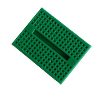
Plastic BreadboardBreadboards are a simple solution for circuit building, especially when you need to prototype or test a circuit. Constructed of plastic, a solderless breadboard contains hundreds of spring-loaded connection sockets (also called tie points) which connect the leads for through-hole electronic components and 22 AWG wire to form an electronic circuit. One key feature of breadboards is that they require no solder to connect your components making testing or prototyping a circuit very quick and painless.

How do breadboards work?

A breadboard is constructed on hundreds of holes arranged in vertical and horizontal rows. The outer rows which run lengthwise across the circuit board are generally reserved for the circuit’s power supply. The interior rows of holes are where the electronic components are inserted. Each row of holes forms a node; that is, any components that reside on the same node will be connected when they are inserted into a hole in that same row, or node. This is because under each row is a copper plate that connects the holes to each other.