Tag Archives: MOSFET

Using Integrated Power Switches

Power switches are most commonly in demand for their simplicity in turning on and off a voltage rail or for protecting a power path. Engineers find load switches easier to use compared to discrete power MOSFETs. For complete power protection of the system, eFuses offer an integrated approach. The combination of load switches and eFuses offers more than significant PCB space savings. Compared to discrete circuits, the combination of load switches and eFuses, also known as integrated switches, offers substantial improvements in performance, while resolving common power management challenges such as faster current limiting, detecting, and responding to mistakes in field wirings, and improving battery life and power density.

In fact, using the right integrated switch helps to reduce EMI and heat generation, while improving the power efficiencies to 90%. Bad power management leads to several side effects such as the generation of excess heat, electromagnetic interference, inaccurate voltage control, and these can lead not only to poor device performance but even to its outright failure. For the above reasons, designers are using integrated switches in electronic equipment such as desktop computers, LCD TVs, and plasma TVs.

Using integrated power switches offers several advantages over solutions of discrete controller and MOSFET. The loser component count leads to lower cost and higher reliability.

With electronic products shrinking in size, PCB space is almost always at a premium. The integrated power switch with its lower footprint has a better advantage over discrete components. Several manufacturers offer a variety of integrated power switches, and these include Fairchild Semiconductors, Power Integrations, ON Semiconductors, and ST.

Fairchild Semiconductor offers their new Green FPS e-Series of integrated switches as a replacement for conventional, flyback converters using hard switches. The new e-Series are a versatile set of devices for improving efficiency by reducing switching losses in the MOSFET with quasi-resonant operation.

It is also possible to use the e-Series in the continuous conduction mode or CCM in fixed frequency operations. The design offers simplicity and lowers the ripple current. Using an advanced burst mode technique, devices of the e-Series also conform to several governmental agency requirements for standby efficiency.

Fairchild uses a prefix of FSQ in the part number of these devices, and they are available for applications that can deliver up to 90 W. Depending on the requirement, it is possible to avail the series in seven different packages including DIP, TO-220F, LSOP, and others.

The devices use valley switching along with inherent frequency modulation for the quasi-resonant operation. The improves efficiency while reducing the EMI signature of the power supply. Valley switching uses the natural resonance of the primary inductance of the transformer and both circuit capacitance and parasitic capacitance for turning the MOSFET on only when the drain-to-source voltage is at its minimum. This reduces the amplitude of the current spike at turn-on typically found in hard-switched converters.

The increased efficiency from reducing the turn-on current spike also reduces the stress on the MOSFET.  However, with valley switching, the power supply can operate with a variable switching frequency, changing with changes in the line and load conditions, helping to reduce the EMI the power supply generates.

Transistors: What Is The Difference Between BJT, FET And MOSFET?

BJTs, FETs and MOSFETs are all active semiconductor devices, also known as transistors. BJT is the acronym for Bipolar Junction Transistor, FET stands for Field Effect Transistor and MOSFET is Metal Oxide Semiconductor Field Effect Transistor. All three have several subtypes, and unlike passive semiconductor devices such as diodes, active semiconductor devices allow a greater degree of control over their functioning.

Depending on their subtypes, operating frequency, current, voltage and power ratings, all the three types of transistors come in a large variety of packages, and all of them are susceptible to ESD or Electro Static Discharge. That means when you handle these devices, you must take adequate precaution against static charges destroying them.

he basic construction of a BJT is two PN junctions producing three terminals. Depending on the type of junctions, the BJT can be a PNP type or an NPN type. The three terminals are identified as the Emitter or E, the Base or B and the Collector or C. BJTs usually function as current controlling switches. The three terminals can be connected in three types of connections within an electronic circuit – Common Base configuration, Common Emitter configuration and Common Collector configurations. All the three connections have their own functions, merits and demerits. The BJT is Bipolar because the transistor operates with both types of charge carriers, Holes and Electrons.

The FET construction does not have a PN junction in its main current carrying path, which can be made from an N-type or a P-type semiconductor material with high resistivity. A PN junction is formed on the main current carrying path, also called the channel, and this can be made of either a P-type or an N-type material. The three leads of a FET are the Source (S), Drain (D) and Gate (G), with Source and Drain forming the ends of the channel and the Gate controlling the channel conductivity. Unlike the BJT, the FET is a unipolar device since it functions with the conduction of electrons alone for the N-channel type or on holes alone for a P-channel type.

The input impedance at the gate of an FET is very high, unlike the BJT, which comparatively has much lower impedance. Additionally, the conductivity of the channel depends on the voltage applied to the Gate, essentially making it a voltage-controlled device, unlike the BJT, which is current-controlled. The voltage applied to the Gate controls the width of the channel, allowing the FET to carry current between the Drain and Source pins. The Gate voltage that cuts off the current flow between Drain and Source is called the pinch off voltage and is an important parameter.

The MOSFET is a special type of FET whose Gate is insulated from the main current carrying channel. It is also called the IGFET or the Insulated Gate Field Effect Transistor. A very thin layer of silicon dioxide or similar separates the Gate electrode and this can be thought of as a capacitor. The insulation makes the input impedance of the MOSFET even higher than that of a FET. The working of the MOSFET is very similar to the FET.

You can read more about transistors in depth here.

BUZ11 – a Popular Power MOSFET

BUZ11

BUZ11

The BUZ11 is an N-Channel enhancement mode silicon gate power field effect transistor designed for applications such as switching regulators, switching converters, motor drivers, relay drivers, and drivers for high power bipolar switchng transistors requiring high speed and low gate drive power. The BUZ11 is also used for DC-DC and DC-AC converters and in the automotive environment for injection, ABS, airbags, lampdrivers and more.

It features:

  • 33A 50V
  • Nanosecond Switching Speed
  • Linear Transfer Characteristics
  • High Input Impedance

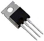
The BUZ11 is in a TO220 package.

If you are looking at the BUZ11 with the drain (flange) at the top, the left pin is the GATE, the middle is the DRAIN, and the right lead is the SOURCE.