Category Archives: IC’s

The Energy Efficient RRAMs

Engineers at Stanford are making 3-D memory chips that can offer faster and more energy efficient solutions for computer memory. These are the Resistive random Access Memory or RRAMs, which are based on a new semiconductor material. It stores data based on temperature and voltage. However, the actual workings of RRAMs continued to be a mystery until a team at Stanford used a new tool for their investigations. They found the optimal temperature range to be lower than they had expected. This could lead to memory that is more efficient.

Conventional computer chips operate on a two dimensional plane. Typically, the CPU and memory communicate with each other through the data bus. While both the CPU and memory components have advanced technically, the data bus has lagged, leading to a slowdown of the entire system when crunching large amounts of data.

The special semiconductor RRAMs can be stacked one on top of the other, creating a 3-D structure. This brings the memory and its logic components closer together. As conventional silicon devices cannot replicate this, the 3-D high-rise chips can work at much higher speeds and be more energy efficient. Not only is this a better solution for tacking the challenges of Big Data, it can also extend the battery life of mobile devices.

The RRAMs work more like a switch. As explained by the Stanford engineers, in their natural state, the RRAM materials behave just as insulators do—resist the flow of electrons. However, when zapped with an electric field, a filament-like path opens up in the material, and electrons can flow through it. A second jolt closes the filament, and the material returns to being the insulator it was. Alternating between the two states generates a binary code with no signal transfer representing a zero and the passage of electrons representing a one.

The temperature rise of the material when subjected to the electric field causes the filament to form, allowing electrons to pass through. So far, the engineers were unable to estimate the exact temperature of the material that caused the switch. They needed much more precise information about the fundamental behavior of the RRAM material before they could hope to produce reliable devices.

As the engineers had no way of measuring the heat produced by a jolt of electricity, they heated the RRAM chips using a hot plate, while not applying any voltage. They then monitored the flow of electrons as filaments began to form. This allowed the team to measure the exact temperature band necessary for the materials to form the filaments. The engineers found the filaments formed between 26.7 and 126.7°C. Therefore, future RRAM devices will require less electricity for generating these temperatures, and that would make them more energy efficient.

Although at this moment, RRAMs are not yet ready to be incorporated into consumer devices, the researchers are confident that the discovery of the temperature range will speed up development work.

According to Ziwen Wang, a member of the team, the voltage and temperature discovered can be the predictive design inputs for enabling the design of a better memory device. The researchers will be presenting their find at the IEEE International Electron Devices Meeting in San Francisco.

AT21CS01 from Atmel: This EEPROM Does Not Require External Power Source

AT21CS01 from Atmel is a two pin serial EEPROM. Astonishingly, it does not have a Vcc or power supply pin characteristic of any IC and does not require an external power source to work. This amazing memory IC operates with only a data pin and a ground pin. The memory in the IC is organized as 128×8 bits, that is, a total of 1-kbits.

The single-wire device, AT21CS01, operates with only an SI/O and GND pin. The SI/O signal functions as a combination of data and power line. That means, apart from moving data in and out of the IC, the SI/O pin also provides power to the device. During high time of the protocol sequence, the IC’s parasitic power scheme provides the IC with power.

Each AT21CS01 is factory programmed to include a unique serial number of 64-bits. The SI/O line can be accessed directly from outside the application, because the device complies with the IEC 61000-4-2 ESD tolerance. This memory IC comes in 4-ball WLCSP, 8-lead SOIC and 3-lead SOT23 packages. Market availability is slated for the fourth quarter of 2015.

Possible applications for AT21CS01 include ink and toner print cartridge identification, storing data for analog sensor calibration and management of after-market consumables. There are several advantages in using AT21CS01.

Manufacturers claim AT21CS01 consumes 33% lower power in its active mode when compared to devices offered by the competition. For instance, at 25°C, the typical write current for an AT21CS01/11 is 200 µA, the typical read current measures about 80 µA, and a typical standby current of 700 nA. Each memory location can endure 1 million write cycles.

With such features, the AT21CS01 is eminently suitable as identification markers for cables, batteries, consumables, wearables and IoT. To support different voltage requirements, the AT21CS01 comes in two variants. AT25C501 is suitable for applications operating in the range of 1.7 to 3.6V. However, when operating with Li-Ion or polymer batteries, applications require higher voltage ranges, such as 2.7 to 4.5V, for which, the AT21C511 is suitable.

With its ultra-low active and standby currents, the AT25C501 beats the competition by consuming at least one third less power. The single-wire interface follows the I2C communication protocol. This IEC 61000-4-2 Level 4 ESD compliant device can withstand discharges of +8KV in contact and +15KV in air.

The innovative memory is organized into for zones of 256-bits each, with a security register additional to the 1 Kb memory space. Each EEPROM has a 64-bit serial number programmed at the factory and includes 16-bytes extra for user programmability. That means the user can improve on the uniqueness of the serial number on each device.

The advantages of using AT25C501 are many. The designer needs only one pin from the ASIC/MPU/ASSP/MCU. Because of its smaller footprint, layout is simple and the consumed PCB area reduces. That makes it easy to integrate identification capabilities in cables and or consumables. Its lower energy consumption is a boon for instruments working on batteries. The high-speed mode of AT25C501 even in low power applications results in high performance.

Why Do ICs Need Bypass Capacitors?

Any electronic design engineer will vouch for the necessity of supplementing integrated circuits on their PCB with bypass capacitors, although they may not understand the reason to do so very well. As a rule of thumb, engineers provide every IC with a 0.1µF ceramic capacitor next to its power pins in each circuit board they design. Along with proper PCB layout techniques, adding a bypass capacitor improves circuit performance and maximizes the efficacy of the ICs.

The trouble lies with transition currents. Circuits handling digital signals produce rapid transitions when their signals switch states. When digital circuits output a high state, the signal voltage is very close to the supply voltage. When they output a low state, the signal voltage reaches very near the ground voltage. When transiting from a low to high or a high to low, the voltage swing from supply to ground or from ground to supply, causes a transient current to be drawn from the supply.

Usually, power to an electronic circuit on a PCB is fed at a single point and traces on the PCB carry this power to each IC. Traces on the PCB have their own parasitic inductance, which, when coupled with the source impedance of the power supply, react to transient currents by creating voltage transients.

The trouble aggravates when ICs have to drive low-resistance or high-capacitance loads. The low-resistance demands high currents when the digital state changes from low to high. Again, when the digital state changes from high to low, there is a demand for the load current to reduce suddenly. However, according to Lenz’s Law, an induced current will flow such as to oppose the change that produced it.

The net effect of transient currents and the parasitic inductance of PCB traces and wires are to create high-magnitude voltage transients, ringing or severe oscillations in the power lines. This can lead to suboptimal circuit performance or even to system failure. Engineers at Texas Instruments have demonstrated an improperly bypassed line driver IC switching at 33MHz can induce ringing amplitude of the order of 2V peak-to-peak on a 5V power rail.

Placing a 0.1µF ceramic capacitor close to the IC power pins improves the situation, because capacitors store charge. Placing the bypass capacitor close to the IC allows low resistance and series inductance. The bypass capacitor is therefore in a better situation to supply or absorb the transients on the PCB traces, which have a comparatively larger resistance and series inductance.

Although engineers refer to such components as both bypass and decoupling capacitors, there is a subtle distinction between the two terms. Decoupling refers to the amount by which one part of the circuit influences another. Bypassing provides a low-impedance path allowing noise to pass by an IC on its way to ground. A capacitor, placed close to the IC supply pins, accomplishes both decoupling and bypassing. However, a decoupling capacitor has an additional task. It blocks the DC component of a signal and prevents it from traveling through to the next part of the circuit, while allowing the AC component little or no resistance at all.

How Does Switching Affect Semiconductors?

Even though ICs rule the world of electronics, the transistor does all the work. Within each IC are millions upon millions of transistors perpetually switching on and off so that the IC can carry out its intended functions. Even if one of the multitudes of transistors were to stop switching, the IC could lose part or all of its functionality.

Circuits handling digital signals most often use transistors to switch from a high state to a low state and vice versa. It is usual to call a circuit point as being in a high state if the voltage at that point is close to the supply voltage. If the circuit point is closer to the ground or zero voltage, we generally call it as being at a low state. The time taken for the transistor to switch from a high to a low state or vice versa is its switching rate. While the transistor does not expend much energy when at either the low or the high state, the same cannot be said for the time when it is actually switching.

Under ideal conditions, a transistor should switch instantaneously. That means the transistor should take zero seconds to change its state. However, ideal conditions do not happen in reality and the transistor takes a finite time, however small, to actually switch over.

Transistors are made of semiconductor material and each junction has a finite capacitance and resistance. Junction capacitances store energy and the combination of resistance and capacitance acts to slow down switching – the capacitance must fill up or empty itself before the transistor can flip. The rate at which the capacitance fills up or empties itself depends on the junction resistance.

The situation gets worse as the switching frequency goes up. As the transistor is driven to toggle faster and faster, the junction capacitance may not get enough time to discharge or charge up fully. That defines the maximum switching rate the transistor can achieve.

Semiconductor manufacturers use various methods to reduce junction capacitances and resistances to induce these special semiconductors switch faster. Although modern semiconductors (transistors and diodes) are capable of switching at MHz or GHz scales, the cumulative effect of the tiny switching losses add up to increase the junction temperature.

Power is the product of voltage and current. When a semiconductor is in a high state, although the voltage is high, the current is negligible and consequently, the power drawn from the supply is negligible. When the semiconductor is a low state, its voltage is close to the ground level and the product of current and voltage is again negligible.

However, during switching, when the voltage is somewhere in-between the supply and ground levels, the current drawn also increases. That makes the product of voltage and current have a significant value and the semiconductor generates heat because of the power consumption. With higher frequencies, this happens more frequently and the heat accumulates to produce higher junction temperature.

If the natural process of heat dissipation can remove the accumulated heat, the semiconductor soon reaches a steady temperature. Else, heatsinks and or forced cooling methods are necessary to remove the heat accumulated.

What is Emitter-Coupled Logic?

When multiple digital signals have to be combined, engineers use several types of logic gates. One of the most popular and widely used types of logic gates made of transistors is called the Emitter-Coupled Logic or ECL. It makes use of a transistor-based differential amplifier to amplify and combine digital signals. Usually, these circuits or gates, as they are commonly known, have multiple inputs and most are single output. Circuit design ensures that none of the transistors in the gate ever saturates nor are they completely turned off. That means the transistors are always working in their linear active operational region and therefore, do not have to contend with a charge storage time. That makes these gates work at extremely high speeds and this is the main advantage of Emitter-Coupled Logic gates.

For example, consider a three-input OR/NOR gate from the Motorola series of MECL devices. This circuit works on standard voltages of -5.2V (VEE) and ground (VCC). Any unused inputs have to be tied to VEE to prevent erratic behavior. The bias circuit is made up of transistors and associated diodes and resistors (not shown). The circuits are generally packaged as integrated circuits as multiple gates in a single IC. Typically, such ICs include quad 2-input, triple 3-input and dual 4-input gates. Here, the gates differ only in the number of input transistors they are built of, while a single bias circuit suffices for all the gates.

While in operation, a logic output changes its state from a high of -0.75V to a low of -1.60V, a change of only 0.85V. The differential amplifier transistors receive a fixed bias of -1.175V from the internal bias circuit. Now, if all inputs are at -1.6V or tied to the VEE rail, the input transistors are turned off, with the internal differential transistors alone conducting current. This causes the base voltage of the OR output transistor to reduce and its output voltage remains at -1.6V. Simultaneously, since none of the input transistors is affecting the base of the NOR transistor, its output rises to -0.75V, which is the emitter-base voltage VBE of the transistor itself. All transistors in the IC are designed to show a VBE of 0.75V.

As soon as an input rises to -0.75V, that transistor draws emitter current away from the internal differential transistors. This causes the outputs to switch states. Although these circuits work with very small voltage changes, which are typically dictated by the VBE of the internal transistors, the current flowing through various parts of the circuit is of greater importance. This is why Emitter-Coupled Logic has another name – Current Mode Logic or CML. Many other logic types also implement the CML and all of them suffer a major drawback – they draw a great deal of current from the power supply and tend to dissipate heat to a significant amount.

To counter this drawback, other logic systems have evolved, such as TTL and CMOS. For example, high-speed devices such as frequency counters employ ECL only at the input ends of their circuitry, following it up with high-speed CMOS or TTL counters at later stages.

Different Types of Digital Logic Gates

digital logic gates explained
In the presence of different digital signals that need to be combined to make a logical decision, engineers use different types of digital logic gates. Usually, these gates have several inputs but a single digital output. Where a larger logic gate function or a sequential or combinational circuit is required, it is usual for individual logic gates to be connected together.

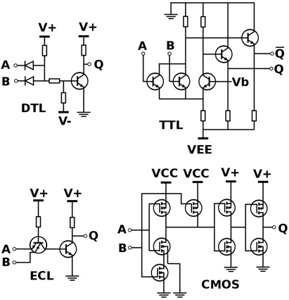
Digital logic gates in standard commercial form are available in two basic forms or families – TTL or Transistor-Transistor Logic and CMOS or Complementary Metal-Oxide-Silicon. An example of the TTL types is the 74xx family and the 4xxx family for the CMOS types. The notation TTL or CMOS is the logic technology that manufacturers use for the Integrated Circuit or IC or chip as commonly known.

The difference in the two families depends on the type of transistors used in making these ICs. While ICs using the TTL logic make use of PNP and NPN type of Bipolar Junction Transistors, the CMOS logic uses JFET or complementary MOSFET type of Field Effect Transistors for their input as well as output circuits.

Apart from the TTL and CMOS technologies, other simpler types of Digital Logic Gates also exist. Some involve the use of diodes, resistors and transistors strung together as RTL or Resistor-Transistor logic gates. Other types are DTL or Diode-Transistor logic and ECL or Emitter-Coupled logic. However, these are far less common compared to the popular TTL and CMOS family, owing to the lower power consumption and heat dissipation of the latter types.

It is usual for ICs to be grouped together into families based on the number of gates or transistors they contain. For example, a single OR gate may be made up of only a few individual transistors, whereas complex micro-controllers have several thousands of individual transistor gates. This leads to integrated circuits being classified as Small Scale Integration or SSI, Medium Scale Integration or MSI, Large Scale Integration or LSI, Very-Large Scale Integration or VLSI, Super-Large Scale Integration or SLSI and Ultra-Large Scale Integration or ULSI. Most complex micro-controllers, video processors, GPUs, CPUs, PICs & FPGAs are examples of ULSI containing several million transistors.

The most modern level of integration, representing the increasing complexity of modern digital circuits, is the Systems-on-Chip or SOC. Here, a single piece of silicon forms the base for individual components such as IO logic, peripherals, memory and the microprocessor. This represents a complete electronic system within the individual single chip.

The Digital Logic Gate forms the basic building block for construction of the entire field of digital electronic circuits and all microprocessor based systems. Digital Logic Gates fundamentally perform logical operations such as AND, OR and NOT on binary numbers represented by digital voltage signals.

The digital logic design recognizes only two voltage levels or states. These are generally referred to as the True, High or Logic “1” and False, Low or Logic “0” states. In Boolean algebra and in standard truth tables, the digits “1” and “0” represent the two states. In terms of voltages, digital logic systems typically use a “Positive Logic”. Here, the level “0” is represented by 0V or ground potential and a higher voltage such as 1.8V or 3.3V or 5.0V represents level “1”.

Versatile Chip to Convert Temperature to Bits Directly

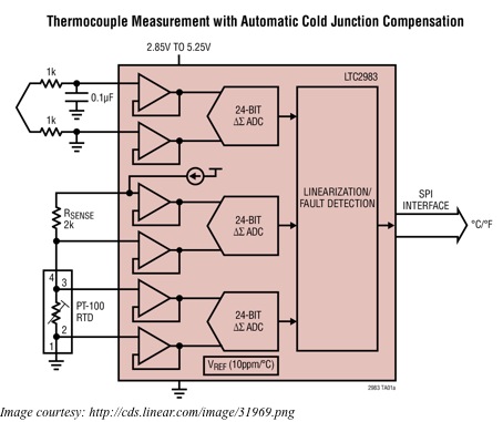
LTC2983One of the most fundamental aspects of our lives is temperature. As yet, measuring temperature accurately is difficult. Galileo was possibly the first person to have invented a thermometer that could measure changes in temperature. Two hundred years after Galileo, Seebeck discovered the principle of thermocouples – a device that generates a tiny voltage related to temperature gradients in dissimilar metals. Today, we use many elements such as semiconductor elements and temperature dependent resistive elements for measuring temperature electrically.
Most temperature measuring elements are analog devices. Digitization of these analog devices leads to measurement of temperature with greater accuracy and precision. So far, this was achievable only with expertise in analog and digital circuit design. However, a versatile chip is now available that helps to convert temperature directly to the required digital bits.

The LTC2983 carries within itself all the analog circuitry that different sensors need. It also has the necessary temperature measurement algorithms and data for linearization so that each sensor can measure temperature directly and the LTC2983 can output the results in degrees Centigrade. The IC makes it easy to handle all the challenges unique to diodes, thermistors, RTDs and thermocouples.

For example, a thermocouple will generate a voltage when there is a temperature difference between its tip and its cold junction – the tip touches the surface whose temperature is to be measured, while the cold junction is on the circuit board. Now, for an accurate measurement of the thermocouple temperature, you also require an accurate measurement of the temperature of the cold junction. A separate non-thermocouple temperature sensor, placed at the cold junction, usually does that.

With the LTC2983, you can connect diodes, RTDs or thermistors to measure the cold junction temperature. To convert the voltage output from the thermocouple into temperature, one has to solve a 14th order polynomial equation for both the voltage from the tip as well as from the cold junction. The advantage with the LTC2983 is that it has the required polynomials built into it for all the eight standard types of thermocouples – J, K, N, T, R, S and B – used in the industry. Therefore, not only does the LTC2983 measure the thermocouple output and the cold junction temperature, it also performs all the required calculations for reporting the thermocouple temperature in degrees Centigrade.

Thermocouples usually generate less than 100mV at full-scale output. Voltages at such low levels require the Analog to Digital Converter to have very low offset and noise. Furthermore, the reference voltage needed for the absolute voltage reading requires good accuracy and low drift. The 24-bit ADC within the LTC2983 has all these qualities – its noise and offset is below 1µV, and its reference voltage has a maximum drift of 10ppm/°C.

If the tip of the thermocouple is exposed to temperatures below that of the cold junction, the voltage output goes below the ground level. This complicates matters, as the circuitry requires an additional negative supply or circuitry that can shift the input level. The LTC2983 handles all this with a single ground-referenced supply, as it incorporates a front-end that can digitize signals below ground. In addition, the LTC2983 has high input impedance, low input currents and is able to accommodate external protection resistors and filtering capacitors.

How to Select Voltage References

how to select voltage referencesSensing applications use Analog to Digital Converters and Digital to Analog Converters and the accuracy of their readings depends on the voltage reference used. Most often the voltage reference used are very simple components with only two or three pins. However, the performance of these references depends on several parameters and careful attention is necessary when selecting the proper one. Typically, applications use either a shunt or a series voltage reference.

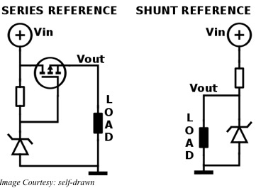
A series voltage reference is basically a high precision, low-current linear regulator. The load current comes through a series transistor positioned between the input voltage and an internal reference voltage. For the shunt voltage reference, a transistor placed parallel to the load shunts excess current to ground. As the series reference has to supply only the required load current, the shunt reference dissipates more power. The bias current of a shunt reference has to be greater than or equal to the maximum load current plus the minimum operating current of its internal reference.

In general, shunt references offer the user greater flexibility in handling higher input voltages and in creating floating or negative references. They also provide better power supply rejection but consume higher power. On the other hand, series references dissipate lower power and perform better for high-precision applications. The typical way of depicting the use of a shunt reference is by showing the symbol of a Zener diode.

Drift or variation of the reference voltage over temperature is a very important factor and has the units of parts-per-million per degree Celsius or ppm/°C. Most monolithic references use the bandgap reference as their base. Special circuitry is required to maintain drifts lower than 20 ppm/°C with the additional circuitry providing some form of curvature correction. Other types of references use a buried Zener diode voltage combined with the base-to-emitter voltage of a bipolar transistor to provide a stable reference voltage of about 7V. Both types have similar drift characteristics, but buried Zener types offer better noise performance.

All voltage references generate internal noise producing a dynamic error degrading the signal to noise ratio of a data converter. Device datasheets typically provide specifications separately for low and for high frequency noise in addition to the broadband noise in rms microvolts over the 10 Hz to 10 KHz bandwidth. You can reduce the broadband noise by adding a bypass capacitor.

Thermal cycling or change in temperature causes references to show thermal hysteresis. This appears as a shift in the reference voltage. Manufacturers define a thermal cycle as an excursion from room temperature to a minimum and a maximum temperature with a return to the room temperature. This is important as the reference may have to be soldered and this can induce shifts from the desired reference voltage.

Continuous operation may cause long-term stability issues resulting in a typical shift in the reference voltage. Manufacturers usually state the shift after six weeks or 1000 hours of continuous use. Since long-term stability is typically related logarithmically to time, the shift in reference voltage in the first 1000 hours provides a rough idea of the stability of the voltage reference over its life.

DC-DC converter with increased efficiency & reduced noise

The new Synchronous Buck-Boost DC/DC converter LTC3111 available from Linear Technology is very significant in many respects. The most important factor being that it is able to operate at 95% efficiency and that too at a very low noise level. It can give a power output of 1.5A when used from a very wide range of power sources. These include multiple or single cell batteries, wall adapter and super-capacitor stacks. This convertor accepts 2.5 to 15V as the input and outputs 5V with the regulated output converted at almost 95% efficiency. Its noise reduction technology ensures that LTC3111 operates at a reduced level on a continuous basis at both buck or boost transitions. This convertor is considered ideal for all applications that require power output at a constant level without noise when the input is varying.

In many areas of operation, where battery life is to be extended by step down solutions, this convertor offers a straightforward solution. This is done by synchronizing the default 800KHz frequency to an external 600 KHz to 1.5 MHz clock. LTC3111 has a proprietary feature of the third generation that gives maximum efficiency at a very low noise level. That reduces the use of external components, which makes the solution offered extremely compact in all respects.

The LTC3111 has four N-channel MOSFETs with very low on-state resistance and the efficiency of 95% is achieved with the use of a single inductor. The Burst Mode is user selectable and this operation impressively lowers the quiescent current down to only 49µA. That enhances the light-load efficiency and significantly improves the battery run time. The burst mode has the option of being disabled whenever the operation is for noise sensitive applications. The output can be disconnected from the load; it has over voltage protection and short circuit protection. A thermal shutdown feature is one of the main advantages of this LTC3111 convertor.

These converters are offered in the market with several variations in packaging. The 14-lead 3mmx4mm DFN package is identified as LTC 3111EDE. Thermally enhanced 16 lead packages are also available and identified as LTC3111MSE. The pricing has been kept competitive. The industrial grade component with an operating junction temperature range of -40 to 125°C is priced slightly on the higher side. Further, higher operating temperature convertors that range from -40 to 150°C are also being offered at special prices. The same converter versions with high reliability are also on offer. Their operating temperature range is from -55 to 150°C. Most significantly, all the versions are available for immediate shipping and discounts are given for bulk quantities.

Notably, the Synchronous Buck-Boost DC/DC converter LTC3111 launched by Linear Technology is significant for both industrial and domestic applications. It is able to achieve an optimum output of 95%, even when the power input is from different sources. The noise level is also considerably reduced as compared to other similar products in the market. This converter is the answer for optimum performance for all noise-sensitive applications. With ready-to-ship availability, this product will find a number of users.

Demystifying the A/D and D/A Converters

Analog and Digital Signals

Analog signals represent a physical parameter in the form of a continuous signal. In contrast, digital signals are discrete time signals formed by digital modulation. Most natural signals, like human voice and other sounds are analog in nature. Traditionally, communication systems were based on analog systems.

As demand for systems capable of carrying more information over longer distances kept soaring, the drawbacks of analog communication systems became increasingly evident. Efforts to improve the performance and throughput of systems saw the evolution of digital systems, which far surpasses the performance of analog systems, and offer features that were considered impossible earlier. Some major advantages of digital systems over analog are:

• Optical fibers can transmit digital signals and have virtually infinite information bearing capacity
• Combining multiple input signals over same channel is possible by multiplexing
• Digital signals can be encrypted and hence are more secure
• Better noise immunity leads to superior performance due to regeneration
• Much higher flexibility and ease of configuration

On the other hand, disadvantages include:

• Higher bandwidth required to transmit the same information
• Accurate synchronization required between transmitter and receiver for error free communication

Primary signals like human voice, natural sounds and pictures, etc., are all inherently analog. However, most signal processing and transmission systems are progressively becoming digital. Therefore, there is an obvious need for conversion of analog signals to digital. This facilitates processing and transmission, and reverse transition from digital to analog, since the digital signals will not be intelligible to human receivers or gadgets like a pen recorder. This need led to the evolution of Analog to Digital (A/D) Converters for encoding at the transmitting end and Digital to Analog (D/A) Converters at the receiving end for decoding.

Principle of Working of A/D and D/A Converters

An A/D converter senses the analog input signal at regular intervals and generates a corresponding binary bit stream as a combination of 0’s and 1’s. This data stream is then processed by the digital system until it is ready to be regenerated at the receiver’s location. The sampling rate has to be at least twice the highest frequency of the input signal so that the received signal is a near perfect replica of the input.

In contrast, a D/A Converter receives the bit stream and regenerates the signal by plotting the sampled values to obtain the input signal at the receiving end. The simplest way to achieve this is by using a variable resistor network, which converts each digital level into an equivalent binary weighted voltage (or current). However, if the recipient is a computer or other device capable of handling a digital signal directly, processing by D/A Converters is not necessary.

Two of the most important parameters of A/D and D/A Converters are Accuracy and Resolution. Accuracy reflects how closely the actual output signal resembles the theoretical output voltage. Resolution is the smallest increment in the input signal the system can sense and respond to. Higher resolution requires more bits and is more complicated and expensive, apart from being slower.