 Sensing applications use Analog to Digital Converters and Digital to Analog Converters and the accuracy of their readings depends on the voltage reference used. Most often the voltage reference used are very simple components with only two or three pins. However, the performance of these references depends on several parameters and careful attention is necessary when selecting the proper one. Typically, applications use either a shunt or a series voltage reference.
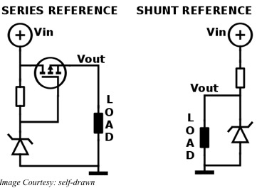
A series voltage reference is basically a high precision, low-current linear regulator. The load current comes through a series transistor positioned between the input voltage and an internal reference voltage. For the shunt voltage reference, a transistor placed parallel to the load shunts excess current to ground. As the series reference has to supply only the required load current, the shunt reference dissipates more power. The bias current of a shunt reference has to be greater than or equal to the maximum load current plus the minimum operating current of its internal reference.
In general, shunt references offer the user greater flexibility in handling higher input voltages and in creating floating or negative references. They also provide better power supply rejection but consume higher power. On the other hand, series references dissipate lower power and perform better for high-precision applications. The typical way of depicting the use of a shunt reference is by showing the symbol of a Zener diode.
Drift or variation of the reference voltage over temperature is a very important factor and has the units of parts-per-million per degree Celsius or ppm/°C. Most monolithic references use the bandgap reference as their base. Special circuitry is required to maintain drifts lower than 20 ppm/°C with the additional circuitry providing some form of curvature correction. Other types of references use a buried Zener diode voltage combined with the base-to-emitter voltage of a bipolar transistor to provide a stable reference voltage of about 7V. Both types have similar drift characteristics, but buried Zener types offer better noise performance.
All voltage references generate internal noise producing a dynamic error degrading the signal to noise ratio of a data converter. Device datasheets typically provide specifications separately for low and for high frequency noise in addition to the broadband noise in rms microvolts over the 10 Hz to 10 KHz bandwidth. You can reduce the broadband noise by adding a bypass capacitor.
Thermal cycling or change in temperature causes references to show thermal hysteresis. This appears as a shift in the reference voltage. Manufacturers define a thermal cycle as an excursion from room temperature to a minimum and a maximum temperature with a return to the room temperature. This is important as the reference may have to be soldered and this can induce shifts from the desired reference voltage.
Continuous operation may cause long-term stability issues resulting in a typical shift in the reference voltage. Manufacturers usually state the shift after six weeks or 1000 hours of continuous use. Since long-term stability is typically related logarithmically to time, the shift in reference voltage in the first 1000 hours provides a rough idea of the stability of the voltage reference over its life.
 Although powerFETs or power Field Effect
