Tag Archives: electronic components

Gardening with the Raspberry Pi

Many of you may be garden enthusiasts and would welcome the idea of automating some of the maintenance requirements of your plants. For example, keeping tabs on the quantity of water that is required by the plants based on the moisture in the soil, the available sunlight and the environmental temperature might be easy for an experienced gardener. However, gardeners who have just started gardening find it a difficult equation to balance. Even an experienced gardener may have to depend on a novice if taking leave from his garden for a few days.

With a Raspberry Pi (RBPi), most of the above gardening issues can be fixed. The Raspberry Pi can take care of the garden’s watering requirements based on a few environmental measurements. This can bring relief to an experienced gardener forced to leave his beloved plants for a few days. The novice gardener can quit worrying if he is starving his plants or drowning them in water. This is how Devon approached the problem with his Raspberry Pi.

Avid gardening enthusiasts know that too much water to a plant can be as bad as too little. For the Raspberry Pi to determine how much water should be delivered to the plant, it is necessary to know how much moisture is present in the soil in the first place. That, combined with the temperature and the amount of available light can let Raspberry Pi control the pump that delivers the water to the garden.

Since Raspberry Pi is not capable of measuring analog signals that most sensors put out, an Analog to Digital Converter attachment is necessary. For this, using the MCP3008 ADC is a good choice since it allows eight sensors to be used at a time. For sensing the amount of sunlight available, a Light Dependent Resistor or LDR is useful. To measure the ambient temperature with some amount of precision, a temperature sensor such as the TMP35 or TMP37 will do. For sensing humidity in the soil, a homemade humidity sensor using a few long metal nails will be fine.

All the sensors will need a DC voltage supply and a return ground connection, with the signal from each sensor going to one of the channels of the ADC. The 3.3VDC from the Raspberry Pi board is good enough for the sensors. While only one temperature sensor and one LDR is enough, you may need more than one humidity sensor, depending on how big your garden is.

The humidity sensors check the resistance of the soil between a pair of probes inserted into the ground. As the soil dries up, the resistance increases between the two probes of the humidity sensor. If several such probes are placed at different places in the garden, the Raspberry Pi has a fairly good idea of the state of dryness of the soil in the garden.

The final and most important part of the entire system is the pump that delivers water to the garden. Using a tank and a submersible pump eliminates a whole bunch of issues that many gardeners face. You can experiment with drip-irrigation also if you like the idea. Devon has kindly shared the software and the code used, and you can download them here.

Sensing humidity using advanced technology

An approaching thunderstorm creates a very stuffy environment with oppressively heavy moisture in the air. The presence of water in the air is termed as humidity and this largely affects human comfort. The amount of water vapor influences many physical, chemical and biological processes. In industries, measuring and controlling humidity is critical since it can affect not only the health and safety of personnel, it can affect the business cost of the product as well.

Sleep apnea leads to repeated cessation of breathing during sleep. People, who suffer from sleep apnea, have to wear a mask to prevent nasal collapse. The mask is connected to a Positive Airway Pressure machine that sends pressurized air through the nasal passage of the patient, to prevent it from collapsing. It is important to monitor the humidity of the air the patient receives, keeping it at the appropriate level of comfort to allow the patient to sleep comfortably.

Traditionally, humidity or relative humidity was measured with the wet and dry bulb hygrometers. This method is neither accurate nor convenient in the industrial environment. With advancement in technology, solid-state devices are now available, which measure humidity with very high accuracy, repeatability and interchangeability. Solid-state humidity sensors are generally of two types, capacitive and resistive.

In resistive type humidity sensors, the resistance of the element changes responding to variations in humidity in the environment. The construction is in the form of two intermeshed printed combs, made of a thick film conductor of a precious metal such as gold or ruthenium oxide. The two combs form two electrodes, the space between them being filled with a polymeric film. This film has movable ions whose movement is governed by humidity. The film thus acts like a sensing film whose resistance changes with change in humidity.

The capacitive type of humidity sensor has an Alumina substrate on which the lower electrode is formed using either gold or platinum. A dielectric polymer layer such as thermoset polymer is then deposited on the lower electrode. This layer is sensitive to humidity. On top of this polymer layer, a top electrode is placed, and this is also made of gold or platinum. The top layer is porous and allows water vapor to pass through into the sensitive PVA layer. Moisture enters or leaves the sensing layer until the vapor content is in equilibrium with the environment. This sensor is therefore a type of capacitor whose capacitance changes with the change in humidity.

The arrangement of a hygroscopic dielectric material sandwiched between two pairs of electrodes, forms a capacitor whose value is governed by the dielectric constant of the hygroscopic material and the sensor geometry. At normal room temperatures, the value of the dielectric constant of water vapor is about 80, which is much larger than the constant of the sensor dielectric material. Therefore, as the sensor absorbs water vapor from the environment, it results in an increase in the capacitance of the sensor.

Both the resistive type and capacitive type of humidity sensors are available in the form of small surface mount SMD packages, and pre-calibrated to simplify, speedup manufacturing and reduce the cost for Original Equipment Manufacturers.

Why Are Industrial Sensors Going Wireless?

Industries are increasingly opting for low-power wireless photoelectric sensors with extended range of signals that carry for miles. Such improvements have been made possible with the proliferation of low-power micro-controllers that have boosted the range of the sensors and enhanced their battery life.

In general, wireless sensors conserve and extend battery life by switching themselves off when they are not taking measurements. This allows the sensor to spend most of its time not consuming any power. With this simple technique itself, the battery life of the sensor is boosted by a factor of 100 or more in comparison to that of a continuously powered sensor. However, as the sensor does not sense when it is off, the response time suffers.

To understand how much the battery life can be extended, consider a dry contact wireless sensor that typically dissipates about 100 to 200 µW of power. Such a sensor operates on two AA batteries, which last for five years with the dry contact wireless sensor sampling at 10 times or more every second. In comparison, a powered sensor system can remain on continuously and can respond more quickly. It is also possible to run them at higher power levels to produce a longer wireless range.

To provide reliable and interference-free communication, FHSS or Frequency-Hopping Spread Spectrum techniques are used in industrial wireless sensors. Basically, FHSS switches a carrier rapidly among several possible frequencies, using a pseudorandom sequence. When bound or paired devices communicate with each other, data and control packets are interchanged using these frequency channels randomly, but in a pattern known only to the communicating pair.

Typically, the bandwidth necessary for frequency hopping is much larger than that required for transmitting the same information on just one carrier frequency. However, the transmission takes place only on a small portion of the bandwidth at any given time. Since the effective bandwidth of any interfering signal is the same as that for a narrow carrier, frequency hopping greatly diminishes interference from narrowband sources. Usually, a site survey is conducted before installation of wireless sensors to determine if there is RF interference and whether this is strong enough to be a problem.

Modern wireless sensor systems have a radio master device or gateway that polls all its sensor nodes at specific intervals to ascertain radio communications are still operating. If there is no response from one of the sensors, the system reacts deterministically; the system enters a state to maintain control in a fail-safe way.

The radio master connects to multiple sensors allowing many dozens of wireless sensor nodes to work within a single radio network. Using a TDMA or Time-Division Multiple-Access technique, ensures that all the sensors in the network have adequate time to transmit their data and receive their individual instructions. This effectively eliminates the possibility of multiple sensors trying to communicate simultaneously.

One of the major advantages of using wireless sensors and indicator lights is the elimination of complex cable installation. Rearrangement can easily be done if the plant layout changes. The modern wireless sensor with its own battery, radio and sensor in a single housing, allows higher productivity with real-life status of the production line.

Where Do You Use a Touchless Rotary Sensor?

Most touchless rotary sensors use a magnetic position marker for sensing position. The position marker is attached to the rotating part of the application. It also uses a sensor to measure the angle of the marker. The touch-less rotary sensor uses a magnetism-based technique and does not require physical contact between the marker and sensor. Although other noncontact magnetism-based sensors overcome the limitations of potentiometric sensors that use resistance-based track-and-wiper techniques, they still need a shaft to be attached to the housing of the sensor.

Touchless rotary sensors are the most suitable technology when you have:
• An application that requires measurements through a nonmagnetic plate or wall;
• An application working in extreme environments that necessitate the sensor shaft to be sealed;
• An application where the drive shaft vibrates or has a lot of play;
• An application that necessitates very low friction-torque requirements;
• An application where misalignment can be problematic.

Touchless sensors offer many advantages over conventional sensors. They have lower operating costs, are rugged, reliable, programmable and simple. Although the initial cost does seem higher than the alternatives, it is not always so. The alternatives often require expensive subcomponents such as ball bearings and or expensive precision shaft couplings.

Since the working core of a touch-less rotary sensor is always sealed from the environment, the sensor parts experience no mechanical wear. Although the magnet is exposed, it can be potted with ingress resistant compounds, especially when it is exposed to fluids. The sensor life is usually measured in MTTF or Mean Time To Failure.

There are two types of touch-less rotary sensors, customer programmable and preprogrammed, making it simple for the user. Where safety and is paramount, preprogrammed and pre-calibrated sensors can be used and their functionality cannot be altered. These are also less expensive as the sensors do not require any look-up table for calibration with microprocessors. Where precision and expanded functions are required for quick calibration of star and end angles, customer programmable touch-less sensors may be used.

To operate properly, both the sensor and the position marker attached to the rotating component of the machine must be appropriately sized and positioned. The magnet position markers come in several body styles. You can either screw them into the rotating component or clamp them onto the rotating shaft. The working distance between the sensor and the magnet is important and dictates the best magnet size. For example, if have a shaft with an axial offset in the X-Y direction, you will need a bigger magnet to compensate for the non-linearity and the drop in the axial tolerance band.

You can mount the sensor unit of the touchless rotary sensor system in the traditional servo-type mounts or in the two to four screw mount. The body of the sensor usually has mounting holes and slots and comes with screws for the mounting. This allows the sensor to be rotated and placed in an optimal mounting position before being secured.

Touch-less sensors typically measure rotary movements from 0-360 degrees with repeatability from 0.1-0.12 degrees. The resolution is typically from 10-14 bits. Most of the sensor units are rated to IP69.

How do photovoltaic cells work?

Your calculator probably has a darkish colored panel just above the display. The panel is made up of solar cells that power up your calculator if there is enough light. You may also have seen some solar panels, which people use for charging up their cell phones. Earlier, these solar cells or photovoltaic cells were exclusively used to power the electrical systems of satellites. However, they are now commonly used in less exotic ways as well.

How do photovoltaic cells convert light to electricity? For this, you must understand the way these cells are constructed. A photovoltaic cell has two silicon plates bonded together. Pure silicon is an insulating material and is unable to conduct electricity. This is because of the atomic structure of silicon, which has place for eight electrons in the outermost shell of its atoms. However, there are only four electrons present.

Therefore, when silicon atoms come together, they share their electrons. Each atom shares one electron with its neighbor and they become a pair. That means at any time, four atoms surround each silicon atom, bringing up its catch of electrons to eight on the outer shell. Since all the electrons are now bound up, there is none left free to move about and carry electric charge.

To make the silicon plates able to carry electric charge, one of the two plates must have some free electrons and the other plate must have some holes or lack of electrons. This is done by the process of doping. While making the plates, one of them is given a few phosphorus atoms as impurities. Since phosphorus has five atoms in the outermost shell of its atom, when combining with the silicon atoms, one of its electrons remains unpaired. This makes the silicon plate with the phosphorus impurity have excess electrons and this is called the n-type silicon.

Likewise, the other plate is doped with boron, which has only three electrons in the outermost shell of its atoms. This leaves the combination of silicon and boron atoms with a deficit of electrons and this is called the p-type silicon. This is like a hole, which will readily grab a wandering electron to fill up its vacant space.

Light is essentially a barrage of energetic particles called photons. Photons impart their energy to the surface where they land, which is why you feel warm when you stand in sunlight. If light or photons are allowed to fall on the n-type silicon plate that has extra electrons, they receive the excess energy from the photons. The extra energy allows them to dislodge themselves from their original positions and wander off until they come to the other plate with the holes, where they are eagerly absorbed.

However, the n-type silicon plate that supplied the electrons now has a deficiency of electrons that it must fill up. For electrons to flow, the circuit must be externally completed. This is usually done by connecting a load to the solar cell through external wires. The plate makes up its deficiency of electrons by borrowing them from the connecting wire. In essence, photons drive the electrons through the entire circuit, and that makes the current flow through the solar cell and the load connected to it.

As soon as light falling on the solar cell is removed, the running electrons lose their drive, and the flow of current stops. Although the output from each cell is usually very tiny, by combining them in series and parallel, an impressive amount of power can be generated.

Transistors: What Is The Difference Between BJT, FET And MOSFET?

BJTs, FETs and MOSFETs are all active semiconductor devices, also known as transistors. BJT is the acronym for Bipolar Junction Transistor, FET stands for Field Effect Transistor and MOSFET is Metal Oxide Semiconductor Field Effect Transistor. All three have several subtypes, and unlike passive semiconductor devices such as diodes, active semiconductor devices allow a greater degree of control over their functioning.

Depending on their subtypes, operating frequency, current, voltage and power ratings, all the three types of transistors come in a large variety of packages, and all of them are susceptible to ESD or Electro Static Discharge. That means when you handle these devices, you must take adequate precaution against static charges destroying them.

he basic construction of a BJT is two PN junctions producing three terminals. Depending on the type of junctions, the BJT can be a PNP type or an NPN type. The three terminals are identified as the Emitter or E, the Base or B and the Collector or C. BJTs usually function as current controlling switches. The three terminals can be connected in three types of connections within an electronic circuit – Common Base configuration, Common Emitter configuration and Common Collector configurations. All the three connections have their own functions, merits and demerits. The BJT is Bipolar because the transistor operates with both types of charge carriers, Holes and Electrons.

The FET construction does not have a PN junction in its main current carrying path, which can be made from an N-type or a P-type semiconductor material with high resistivity. A PN junction is formed on the main current carrying path, also called the channel, and this can be made of either a P-type or an N-type material. The three leads of a FET are the Source (S), Drain (D) and Gate (G), with Source and Drain forming the ends of the channel and the Gate controlling the channel conductivity. Unlike the BJT, the FET is a unipolar device since it functions with the conduction of electrons alone for the N-channel type or on holes alone for a P-channel type.

The input impedance at the gate of an FET is very high, unlike the BJT, which comparatively has much lower impedance. Additionally, the conductivity of the channel depends on the voltage applied to the Gate, essentially making it a voltage-controlled device, unlike the BJT, which is current-controlled. The voltage applied to the Gate controls the width of the channel, allowing the FET to carry current between the Drain and Source pins. The Gate voltage that cuts off the current flow between Drain and Source is called the pinch off voltage and is an important parameter.

The MOSFET is a special type of FET whose Gate is insulated from the main current carrying channel. It is also called the IGFET or the Insulated Gate Field Effect Transistor. A very thin layer of silicon dioxide or similar separates the Gate electrode and this can be thought of as a capacitor. The insulation makes the input impedance of the MOSFET even higher than that of a FET. The working of the MOSFET is very similar to the FET.

You can read more about transistors in depth here.

What Are Inductors and How Do They Work

An inductor or an induction coil is a tightly woven coil of wire. Now, you would not expect an ordinary piece of wire to show any special property on passage of current through it. A coil with several loops or turns however, exhibits a remarkable property when current passes through it. The current through the coil creates a magnetic field in the immediate space surrounding the coil. The field stores electrical energy during the passage of current and for a very short while, even if you cut off the current.

Another amazing fact of an inductor coil is that if you place the coil in a varying magnetic field, a current starts to flow through it. The amount of current depends upon the rate at which you change the field.

Bulb and Coil Experiment

You can make out this amazing property of an inductor coil from a simple experiment. Consider a simple circuit with a battery, bulb and a switch. The bulb glows when you close the switch while it stops glowing the moment you open or release the switch.

If you now include a coil of wire wound around an iron bar across the bulb, the bulb will light up as you close the switch. However, instead of glowing at a constant brightness, the intensity of the light changes from bright to dim. If you now open the switch, the bulb does not turn off immediately as you would expect. Instead, the brightness gradually decreases before turning off completely.

Explaining the Observations

You can attribute this curious behaviour to the inductor coil placed across the bulb. When you close the switch, current flows from the battery through the bulb, causing it to glow. At the same time, current flows through the inductor coil too. This generates a magnetic field in the space surrounding the coil. The magnetic field varies in the short time the current builds up. The changing magnetic field induces a current to flow through the coil. However, according to the rules of electricity, this current is opposite to the original current sent by the battery. Hence, the effective current through the coil increases with time, while decreasing that passing through the bulb. This causes the bulb to reduce its glow from bright to dim.

When you open the switch, the magnetic field falls. During the fall of the field, the induced current causes the voltage across the inductor to rise for a moment. This causes the bulb to brighten up briefly. When the current reduces to zero, the bulb turns off.

Inductance

The physical quantity associated with this property is called inductance. The value of this quantity is measured in Henrys. Inductance depends upon four features, which include the number of turns in the coil, the degree of overlap, area of the cross section of the wire and the material of the core inside the coil.

You can increase the inductance by increasing the number of turns and the cross section area of the coil. You may also increase the value by increasing the degree of overlap i.e. by using a tightly wound coil.

Uses of Inductors

You must have wondered how traffic signalling works. Traffic light sensors make use of inductors, which form filter circuits along with capacitors. Inductors are essential components in electronic circuits and devices like receivers, transmitters, oscillators and voltage regulators, as well.

Digital Isolators vs Optocouplers

Industrial equipment may need to operate in a region of strong electromagnetic fields. There can be a sudden surge in the voltage applied to the equipment, which may be hazardous to the user and the gear. It is crucial that you incorporate a reliable isolation system to take of these issues.

Until very recently, the optocoupler was the only practical choice in providing safety isolation for manufacturers of medical and industrial isolated systems. The arrival of digital isolator has however, changed the situation greatly.

Digital isolators offer several advantages over optocouplers. They are more reliable, cheaper and have greater power efficiency compared to the optocouplers.

It is important that you understand the three vital aspects of an isolation system. These are the insulation material, the structure and the method of transfer of data.

Insulation Material

Typical insulation materials are silicon dioxide wafers and thin film of polymers. Optocouplers use polymer films. Digital isolators make use of a particular form of polymer called polyimide. This material serves to increase the efficiency of isolation systems.

Silicon Dioxide is not a very suitable material as an isolator. While you may increase the thickness of polyimide to increase the insulation, you cannot adopt the same method for silicon dioxide. Wafers thicker than 15 micrometers may crack during processing.

Structure

Digital isolators use either transformers or capacitors to transfer data across the isolation barrier. A transformer system has two coils placed side by side. Current flowing through a coil (called the primary coil) gives rise to a magnetic field in the space surrounding the coil. This induces a current to flow in the other coil (called the secondary coil).

A capacitor consists of two metal plates with the space between the plates filled with a non-conductor.

Optocouplers use light emitting diodes (LED) for data transmission.

Transfer of Data

The LED in an optocoupler turns on for logic high state and turns off for logic low state. The device consumes a significant amount of power when the LED is on. Digital isolators do away with this undesirable aspect. The sophisticated circuitry in the system encodes and decodes data at a rapid pace so that the transmission of data involves less power consumption.

A digital isolator using a transformer for data transmission transfers the data from the primary coil to the secondary coil during the pulses of current driving the transformer.

A digital isolator may use radio frequency signals as well, in a fashion similar to the way an optocoupler uses light from an LED. However, since a logic high state causes a continuous transmission of radio frequency signals, this method uses more power.

Digital isolators with capacitors have an advantage in that they consume lower currents for creating coupling electric fields for data transmission.

Ensuring the Correct Combination

It is important to use the right insulating material and the apt method for data transfer depending upon the application.

Since polymers provide more than adequate insulation, they are suitable in most applications. Polyimide insulation is particularly suitable for equipment used in healthcare and heavy industries.

Concerning data transfer, capacitor isolation is adequate for situations requiring just functional and not safety isolation. Isolation systems making use of transformers will serve the purpose of safety as well as functional isolation.

What Is Electromagnetic Interference (EMI) And How Does It Affect Us?

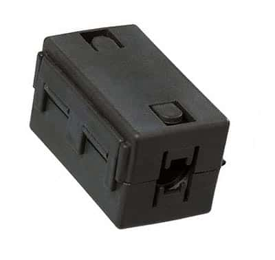
Snap on ferrite for EMI suppression

(Snap on ferrite for EMI suppression)

What Is Electromagnetic Interference (EMI) And How Does It Affect Us?

Electromagnetic interference, abbreviated EMI, is the interference caused by an electromagnetic disturbance affecting the performance of a device, transmission channel, or system. It is also called radio frequency interference, or RFI, when the interference is in the radio frequency spectrum.

All of us encounter EMI in our everyday life. Common examples are:

• Disturbance in the audio/video signals on radio/TV due an aircraft flying at a low altitude

• Noise on microphones from a cell phone handshaking with communication tower to process a call

• A welding machine or a kitchen mixer/grinder generating undesired noise on the radio

• In flights, particularly while taking off or landing, we are required to switch off cell phones since the EMI from an active cell phone interferes with the navigation signals.

EMI is of two types, conducted – in which there is physical contact between the source and the affected circuits, and radiated – which is caused by induction.

The EMI source experiences rapidly changing electrical currents, and may be natural such as lightning, solar flares, or man-made such as switching off or on of heavy electrical loads like motors, lifts, etc. EMI may interrupt, obstruct, or otherwise cause an appliance to under-perform or even sustain damages.

In radio astronomy parlance, EMI is termed radio-frequency interference (RFI), and is a signal within the observed frequency band emanating from other than celestial sources themselves. In radio astronomy, RFI level being much larger than the intended signal, is a major impediment.

Susceptibility to EMI and Mitigation

Analog amplitude modulation or other older, traditional technologies are incapable of differentiating between desired and undesired signals, and hence are more susceptible to in-band EMI. Recent technologies like Wi-Fi are more robust, using error correcting technologies to minimize the impact of EMI.

All integrated circuits are a potential source of EMI, but assume significance only in conjunction with physically larger components such as printed circuit boards, heat sinks, connecting cables, etc. Mitigation techniques include the use of surge arresters or transzorbs (transient absorbers), decoupling capacitors, etc.

Spread-spectrum and frequency-hopping techniques help both analog and digital communication systems to combat EMI. Other solutions like diversity, directional antennae, etc., enable selective reception of the desired signal. Shielding with RF gaskets or conductive copper tapes is often a last option on account of added cost.

RFI detection with software is a modern method to handle in-band RFI. It can detect the interfering signals in time, frequency or time-frequency domains, and ensures that these signals are eliminated from further analysis of the observed data. This technique is useful for radio astronomy studies, but not so effective for EMI from most man-made sources.

EMI is sometimes put to useful purposes as well, such as for modern warfare, where EMI is deliberately generated to cause jamming of enemy radio networks to disable them for strategic advantages.

Regulations to contain EMI

The International Special Committee on Radio Interference (CISPR) created global standards covering recommended emission and immunity limits. These standards led to other regional and national standards such as European Norms (EN). Despite additional costs incurred in some cases to give electronic systems an agreed level of immunity, conforming to these regulations enhances their perceived quality for most applications in the present day environment.

Demystifying the A/D and D/A Converters

Analog and Digital Signals

Analog signals represent a physical parameter in the form of a continuous signal. In contrast, digital signals are discrete time signals formed by digital modulation. Most natural signals, like human voice and other sounds are analog in nature. Traditionally, communication systems were based on analog systems.

As demand for systems capable of carrying more information over longer distances kept soaring, the drawbacks of analog communication systems became increasingly evident. Efforts to improve the performance and throughput of systems saw the evolution of digital systems, which far surpasses the performance of analog systems, and offer features that were considered impossible earlier. Some major advantages of digital systems over analog are:

• Optical fibers can transmit digital signals and have virtually infinite information bearing capacity
• Combining multiple input signals over same channel is possible by multiplexing
• Digital signals can be encrypted and hence are more secure
• Better noise immunity leads to superior performance due to regeneration
• Much higher flexibility and ease of configuration

On the other hand, disadvantages include:

• Higher bandwidth required to transmit the same information
• Accurate synchronization required between transmitter and receiver for error free communication

Primary signals like human voice, natural sounds and pictures, etc., are all inherently analog. However, most signal processing and transmission systems are progressively becoming digital. Therefore, there is an obvious need for conversion of analog signals to digital. This facilitates processing and transmission, and reverse transition from digital to analog, since the digital signals will not be intelligible to human receivers or gadgets like a pen recorder. This need led to the evolution of Analog to Digital (A/D) Converters for encoding at the transmitting end and Digital to Analog (D/A) Converters at the receiving end for decoding.

Principle of Working of A/D and D/A Converters

An A/D converter senses the analog input signal at regular intervals and generates a corresponding binary bit stream as a combination of 0’s and 1’s. This data stream is then processed by the digital system until it is ready to be regenerated at the receiver’s location. The sampling rate has to be at least twice the highest frequency of the input signal so that the received signal is a near perfect replica of the input.

In contrast, a D/A Converter receives the bit stream and regenerates the signal by plotting the sampled values to obtain the input signal at the receiving end. The simplest way to achieve this is by using a variable resistor network, which converts each digital level into an equivalent binary weighted voltage (or current). However, if the recipient is a computer or other device capable of handling a digital signal directly, processing by D/A Converters is not necessary.

Two of the most important parameters of A/D and D/A Converters are Accuracy and Resolution. Accuracy reflects how closely the actual output signal resembles the theoretical output voltage. Resolution is the smallest increment in the input signal the system can sense and respond to. Higher resolution requires more bits and is more complicated and expensive, apart from being slower.